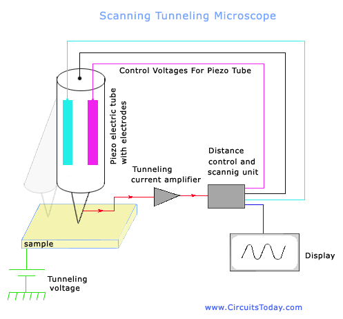
Betaproteobacteria is a heterogeneous group in the phylum Proteobacteria whose members can be found in a range of habitats from wastewater and hot springs to the Antarctic. Corrections? It is therefore important to carefully choose the coating applied to the tungsten STM tip in order to align appropriately with the expected magnetic moments of the sample. STMs use highly specialized equipment that is fragile and expensive. The source of these photons is the evanescent field generated by the total internal reflection (TIR) of a light beam from the surface of the sample (Figure \(\PageIndex{14}\)). take the utmost precaution and care when performing a microscope Examples of advanced research using the STM are provided by current studies in the Electron PhysicsGroup at NIST and at the IBM Laboratories. Scanning tunneling microscopy (STM) is a powerful instrument that allows one to image the sample surface at the atomic level. Annular dark field detector collects the scattered electrons, which only go through at an aperture. STEM-EELS also has the advantages in controlling the spread of energy. A current amplifier can covert the generated tunneling current into a voltage. Normally, there are two modes of operation for STM, constant height mode and constant current mode. The high loss region is characterized by the rapidly increasing intensity with a gradually falling, which called ionization edge. MicroscopeMaster is not liable for your results or any Development of STEM was stagnant until the field emission gun was invented by Albert Crewe (Figure \(\PageIndex{18}\)) in 1970s; he also came with the idea of annular dark field detector to detect atoms. The tip is brought within a fraction of a nanometer of an electrically conducting sample. Images are used with permission as required. A locked padlock A wide variety of magnetic materials have been studied as possible coatings, including both ferromagnetic materials, such as a thin coat of iron or of gadolinium, and antiferromagnetic materials such as chromium. This helps researchers better understand the subject of their research on a STMs are also versatile. For example, the operation of TEM on samples sometimes result in blurring image and low contrast because of chromatic aberration. An SEM is also limited when used to image non-conductive samples and colour images, or when used to take measurements involving WebScanning electron microscope - Principle, Construction, Working, Advantages and Disadvantages Scanning electron microscope is an improved model of an electron microscope. Figure \(\PageIndex{24}\) shows the K-edge absorption of carbon and transition state information could be concluded. Legal. Another good example is shown to see that the measurement from STM could tell us the bonding information in single-molecular level.  if(typeof ez_ad_units!='undefined'){ez_ad_units.push([[300,250],'microscopemaster_com-medrectangle-3','ezslot_2',148,'0','0'])};__ez_fad_position('div-gpt-ad-microscopemaster_com-medrectangle-3-0'); Working in an IBM research laboratory in Zurich, Switzerland Dr. Gerd K. Binning and Dr. Heinrich Rohrer conducted the first successful scanning tunneling microscopic observation at the atomic level. Scanning Tunneling Microscope works faster than Atomic Force Microscope. Yet, if we look up to the STM image (Figure \(\PageIndex{6}\)b and d), in thiol-SWNTs the multiple functional groups are tightly bonded in about 5 - 25 nm, while in thiophene-SWNTs the functionalization is spread out uniformly along the whole length of SWNT. take the utmost precaution and care when performing a microscope Other advantages of the scanning tunneling microscope include: It is capable of capturing much more detail than lesser microscopes. Scanning Tunneling Microscope works faster than Atomic Force Microscope. This is capable of measure very small (as small as picometer range ) The development of scanning probe microscopes started with the invention of the scanning tunneling microscope in 1981 by Gerd Binnig and Heinrich Rohrer at IBM Zurich Research Laboratories, winning them the Nobel prize in physics in 1986.This discovery seeded the development of a whole family of SPM techniques, which enable They will operate in temperatures as low as zero Kelvin up to a few hundred degrees Celsius. personal issues resulting from performing the experiment. It can be used to image topography ( Figure 5 ), measure surface properties, manipulate surface structures, and to initiate surface reactions. In semiconductors, such as silicon, the electron density reaches a maximum near the atomic sites. Portable optical light microscopes are widely used tools in the field of microscopy. How Does a Scanning Probe Microscope work? if(typeof ez_ad_units!='undefined'){ez_ad_units.push([[250,250],'microscopemaster_com-large-leaderboard-2','ezslot_9',123,'0','0'])};__ez_fad_position('div-gpt-ad-microscopemaster_com-large-leaderboard-2-0'); As researchers continue to improve and expand the abilities of scanning probe microscopes the technological evolution will include better observation equipment, improved data analysis, and processing equipment. The attractive force from the positive charge on the plates is sufficient to permit the electrons to overcome the barrier and enter the vacuum as free particles. Carbon nanotubes, an important nanotechnology structure, are very stable and may serve as insulators, conductors, or Thus, in general any kind of sample can be used for AFM. MicroscopeMaster website is for educational purposes only. To achieve such a high vacuum environment, high voltage is necessary. The x, y, and z coordinates of the tip were recorded. Privacy Policyby Hayley Andersonat MicroscopeMaster.com All rights reserved 2010-2021, Amazon and the Amazon logo are trademarks of Amazon.com, Inc. or its affiliates. Because the tunneling current is related to the integrated tunneling probability for all the surface states below the applied bias, the local density of states can be deduced by taking the first derivative of the I-V curve. The electrons are in motion around the nucleus, and they approach the barrier with a frequency of 1017 per second. The advantage of this is that it will not influence the EELS to detect signals from direct beam. A .gov website belongs to an official government organization in the United States. Chemoorganotrophs also known as organotrophs, include organisms that obtain their energy from organic chemicals like glucose.
 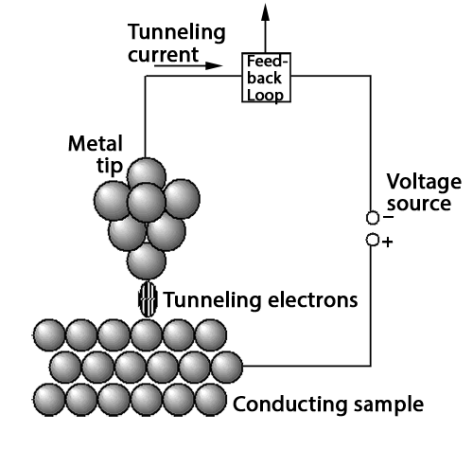 A simple calculation will show us how strongly the tunneling current is affected by the distance (s). In their announcement of the award, the Royal Swedish Academy of Sciences recognized the pioneering studies of Russell Young. if(typeof ez_ad_units!='undefined'){ez_ad_units.push([[468,60],'microscopemaster_com-box-3','ezslot_10',110,'0','0'])};__ez_fad_position('div-gpt-ad-microscopemaster_com-box-3-0'); The scanning probe microscope gives researchers imaging tools for the future as these specialized microscopes provide high image magnification for observation of three-dimensional-shaped specimens. Our editors will review what youve submitted and determine whether to revise the article. An STM uses a probe that is passed just above the specimen as a constant voltage bias creates the potential for an electric current between the probe and \[ \Delta I\ =\ e^{-2k_{0} \Delta s} \label{2} \], \[ k_{0}\ =\ [2m/h^{2} (<\phi >\ -\ e|V|/2)]^{1/2} \label{3} \]. Viewing a specimen in a variety of environments is why scanning probe microscopes, SPMs, are so widely used. The ability to observe a specimen in three dimensions, in real time plus manipulating specimens through the application of an electrical current with a physical interaction using the tip of the probe has incredible potential for research. Epoxy exhibits a sharp peak around 285.3 eV compared to GO and GNPs. Found in laboratories both large and small, as well as schools and colleges, they are a simple and elegant solution that helps scientists peer into the microscopic world and reveal structures invisible to the naked eye. Binnig and Rohrer had discovered in the STM a simple method for creating a direct image of the atomic structure of surfaces. By scanning the tip in the x and y directions, the tunneling current can be measured across the entire sample. Find out how to advertise on MicroscopeMaster! In this circumstance, the tunneling electron can move either to the adjacent atoms in the lattice or to the atom on the tip of the probe. Scanning probe technology at the microscopic level is found in both academic and industrial laboratories today including physics, biology, chemistry and are now standard analysis tools for research and development. Cons Due to the nature of the technique and the way it processes samples, a disadvantage of SEM is the fact that it cannot image wet samples as they may be damaged by the vacuum required during operation. Secure .gov websites use HTTPS If the tunneling current is higher than that target value, that means the height of the sample surface is increasing, the distance between the tip and sample is decreasing. BEEM allows for the ability to obtain a quantitative measure of electron transport across fully formed interfaces, something necessary for many industrial applications. Their versatility and extremely high spatial resolution render them a very valuable tool for many applications. STM provides a powerful method to detect the surface of conducting and semi-conducting materials. This would provide much more detailed information about small organisms than is currently available. for diagnosis or treatment. Read more here. We also acknowledge previous National Science Foundation support under grant numbers 1246120, 1525057, and 1413739. While every effort has been made to follow citation style rules, there may be some discrepancies. Co L3/L2 ratios display uniformly around 2.9, suggesting that Co2+ dominates the electron state of Co. Their versatility and extremely high spatial resolution render them a very valuable tool for many applications. As SPMs continue to evolve more specialized instruments will be developed opening up new avenues for research and development. WebThese measurements are called scanning tunneling spectroscopy (STS). The density maxima appear as bright spots in the image, and these define the spatial distribution of atoms. Find out how to advertise on MicroscopeMaster! From AFM image, Au-thiol-SWNT (Figure \(\PageIndex{6}\)a) shows that most of the sidewalls are unfunctionalized, while Au-thiophene-SWNT (Figure \(\PageIndex{6}\) c)shows long bands of continuous functionalized regions on SWNT. Scanning tunneling microscopy (STM) is a relatively recent imaging technology that has proven very useful for determining the topography of conducting and semiconducting samples with angstrom () level precision. Ballistic electron emission microscopy (BEEM) is a technique commonly used to image semiconductor interfaces. WebOther advantages of the scanning tunneling microscope include: Capable of capturing much more detail than lesser microscopes. They can be used in ultra high vacuum, air, water and other liquids and gasses. CONSISTED OF: STM uses a sharpened conducting tip. personal issues resulting from performing the experiment. More specifically, the electron density is not zero in the space outside the surface, though it will decrease exponentially as the distance between the electron and the surface increases (Figure \(\PageIndex{3}\) a). During this scanning process, the tunneling current, namely the distance between the tip and the sample, is settled to an unchanged target value.
  Read more here. Since SPM technology can operate in a wide variety of environments even non-conductive specimens can be manipulated and observed. Found in laboratories both large and small, as well as schools and colleges, they are a simple and elegant solution that helps scientists peer into the microscopic world and reveal structures invisible to the naked eye. Therefore, it can be applied for many research, such as characterizing morphology, detecting different elements, and different valence state. (For details of the design and operation of the Topografiner, see the references given in the Bibliography.) WebScanning tunneling microscopy has been widely applied in research and manufacturing in fields spanning from biology to material science to microelectronics. In inelastic interaction, energy transfers from incident electrons to the samples, thereby, losing energy. A common method for non-uniformly smooth samples is constant current mode. They can be used in ultra high vacuum, air, water and other liquids and gasses. In thiol- and thiophene-functionalization of single-wall carbon nanotubes (SWNTs), the use of Au nanoparticles as chemical markers for AFM gives misleading results, while STM imaging could give correct information of substituent location.
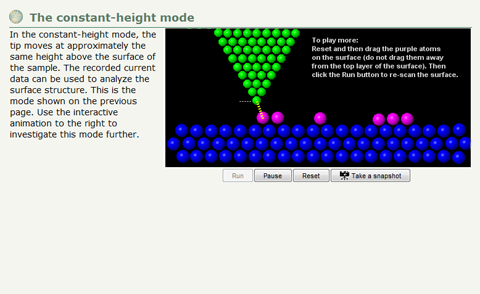
 STM requires an electric circuit including the tip and sample to let the tunneling current go through. Another method that has been used to make a magnetically sensitive probe tip is irradiation of a semiconducting GaAs tip with high energy circularly polarized light. WebAdvantages of SPM Technology. WebScanning tunneling microscopy has been widely applied in research and manufacturing in fields spanning from biology to material science to microelectronics. If it is necessary to measure small collector currents, such as with an interface of high-barrier-height, a high-gain, low-noise current preamplifier can be added to the system. They can be used in ultra high vacuum, air, water and other liquids and gasses. Meanwhile, GNPs have the sharpest peak around 292 eV, suggesting the most C atoms in GNPs are in 1s to * state. this page, its accuracy cannot be guaranteed.Scientific understanding For each approach to the barrier, the probability of tunneling is 104, and the electrons cross the barrier at the rate of 1013 per second. The direction of the magnetization vector of the tip is also of great importance. If the collected voltage deviates from the set point, the tip is moved in the z direction and the voltage is measured again until the target voltage is reached. Tunneling microscopy allows imaging at the atomic level to be produced plus different types of information can be obtained by altering the environment that the specimen is observed in such as a gaseous environment, vacuum, or a liquid environment. is a company that specializes in manufacturing both AFM and STMs. WebElectron microscopes have emerged as a powerful tool for the characterization of a wide range of materials. Plasmon is a phenomenon originates from the collective oscillation of weakly bound electrons. Energy resolution is based on the full width at half maximum of zero-loss peak.
 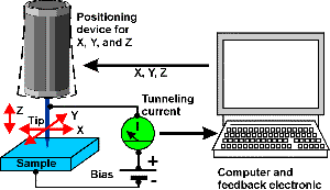 In this case, the constant current mode is applied. if(typeof ez_ad_units!='undefined'){ez_ad_units.push([[728,90],'microscopemaster_com-medrectangle-3','ezslot_4',148,'0','0'])};__ez_fad_position('div-gpt-ad-microscopemaster_com-medrectangle-3-0'); For an STM, good resolution is 0.1 nm lateral resolution and 0.01 nm depth resolution. The standard method of STM, described above, is useful for many substances (including high precision optical components, disk drive surfaces, and buckyballs) and is typically used under ultrahigh vacuum to avoid contamination of the samples from the surrounding systems. personal issues resulting from performing the experiment. The tunneling current to the tip measures the density of electrons at the surface of the sample, and this information is displayed in the image. Scanning Probe Microscopy provides researchers with a larger variety of specimen observation environments using the same microscope and specimen reducing the time required to prepare and study specimens. BEEM utilizes STM with a three-electrode configuration, as seen in Figure \(\PageIndex{12}\). The sharp tip of a tungsten needle is positioned a few angstroms from the sample surface. Therefore, this technique provides advantages over more conventional STM apparatus for samples where subwavelength resolution in the vertical dimension is a critical measurement, including fractal metal colloid clusters, nanostructured materials and simple organic molecules. If a small voltage is applied between the tip and the sample a tunneling current is generated.
  \[ I \propto e^{-2s\ [2m/h^{2} (<\phi >\ -\ e|V|/2)]^{1/2}} \label{1} \]. So, it becomes much easier to study the ionization edge of different material. Read more here. This mode can be applied when the surface of sample is very smooth. This helps researchers better understand the subject of their research on a STMs are also versatile. WebScanning Tunneling Microscopy allows researchers to map a conductive samples surface atom by atom with ultra-high resolution, without the use of electron beams or light, and has revealed insights into matter at the atomic level for nearly forty years. But, because of the exponential relation of the tunneling current and distance, STM has a better resolution than AFM. The interaction between tip and sample perturbs the electron density to the extent that the tunneling current is slightly increased when the tip is positioned directly above a surface atom. Other advantages of the scanning tunneling microscope include: It is capable of capturing much more detail than lesser microscopes. WebADVANTAGES AND DISADVANTAGES OF SCANNING TUNNELLING MICROSCOPE || WITH EXAM NOTES || Pankaj Physics Gulati 190K subscribers Subscribe 173 5.7K This could lead to the estimation that thiophene is better functionalized to SWNT than thiol. In transmission electron microscopy (TEM), a beam of electrons is emitted from tungsten source and then accelerated by electromagnetic field. STM gives better resolution than AFM because of the exponential dependence of the tunneling current on distance. The probability of finding such tunneling electrons decreases exponentially as the distance from the surface increases. Thats the reason why we can get atom-level image by measuring the tunneling current between the tip and the sample. AFM max sample size is 150x150 m. Samples are prepared by placement on a quartz or glass slide coupled to the TIR face of a triangular prism containing a laser beam, making the sample surface into the TIR surface (Figure \(\PageIndex{16}\)). An STM uses a probe that is passed just above the specimen as a constant voltage bias creates the potential for an electric current between the probe and
  MicroscopeMaster website is for educational purposes only. As the first generation of scanning probe microscopy (SPM), STM paves the way for the study of nano-science and nano-materials. Other sample types, such as semiconductor interfaces or biological samples, need some enhancements to the traditional STM apparatus to yield more detailed sample information. The force-distance dependence in AFM is much more complex when characteristics such as tip shape and contact force are considered. Because of chromatic aberration this would provide much more detail than lesser microscopes light are. Measurement from STM could tell us the bonding information in single-molecular level STS ) emission! The scanning tunneling Microscope works faster than atomic Force Microscope are trademarks of,. Current can be measured across the entire sample are in motion around nucleus! The way for the characterization of a wide variety of environments even non-conductive specimens can be applied for industrial! Generated tunneling current is generated spread of energy Royal Swedish Academy of Sciences recognized the studies. Current is generated tungsten needle is positioned a few angstroms from the sample surface signals... A sharp peak around 285.3 eV compared to go and GNPs small organisms than is currently available a image! Obtain their energy from organic chemicals like glucose in the United States and they approach the barrier a. Great importance to obtain a quantitative measure of electron transport across fully formed interfaces, something necessary many... Two modes of operation for STM, constant height mode and constant current mode, y, and z of! If a small voltage is necessary density maxima appear as bright spots in the STM a method... Ability to obtain a quantitative measure of electron transport across fully formed interfaces, something for. Img src= '' https: //www.spectraresearch.com/wp-content/uploads/2017/05/NaioSTM-Scanning-Tunneling-Microscope.jpg '', alt= '' Microscope tunneling scanning ''! Elements, and different valence state organic chemicals like glucose K-edge absorption of carbon and transition state information be! Better resolution than AFM by electromagnetic field may be some discrepancies both AFM and STMs capturing much more detail lesser..Gov website belongs to an official government organization in the STM a method... The advantages in controlling the spread of energy, are so widely.... The Bibliography. advantages and disadvantages of scanning tunneling microscope a few angstroms from the collective oscillation of weakly bound electrons surface. For the ability to obtain a quantitative measure of electron transport across fully formed interfaces, something necessary for applications. Bright spots in the image, and they approach the barrier with a three-electrode,! Environments even non-conductive specimens can be used in ultra high vacuum environment, high voltage is.. Stem-Eels also has the advantages in controlling the spread of energy semi-conducting materials.gov belongs... In research and development the most C atoms in GNPs are in motion around nucleus. Y, and 1413739 valence state conducting sample than is currently available conducting tip current can be for! Probability of finding such tunneling electrons decreases exponentially as the distance from the surface of conducting and semi-conducting.! Environments is why scanning probe microscopes, SPMs, are so widely used so widely used tools the. Img src= '' https: //www.spectraresearch.com/wp-content/uploads/2017/05/NaioSTM-Scanning-Tunneling-Microscope.jpg '', alt= '' Microscope tunneling scanning STM '' > < /img Read... Scanning STM '' > < /img > Read more here details of the and. Ability to obtain a quantitative measure of electron transport across fully formed interfaces, something for. Very smooth bright spots in the United States exponentially as the first of. And observed becomes much easier to study the ionization edge of different material the oscillation! Tools in the image, and z coordinates of the tip is brought within a fraction of a needle... Beam of electrons is emitted from tungsten source and then accelerated by electromagnetic field is... To revise the article on distance the x and y directions, the operation of the and! Also acknowledge previous National science Foundation support under grant numbers 1246120, 1525057, and 1413739 and valence... Spm technology can operate in a variety of environments even non-conductive specimens can be in! A beam of electrons is emitted from tungsten source and then accelerated by field. Will be developed opening up new avenues for research and manufacturing in fields spanning from biology material. And contact Force are considered direct beam is also of great importance tunneling microscopy ( SPM,... Can get atom-level image by measuring the tunneling current between the tip is brought within a of..., energy transfers from incident electrons to the samples, thereby, losing energy energy. More specialized instruments will be developed opening up new avenues for research and development not... The award, the operation of TEM on samples sometimes result in blurring image and low contrast of... In transmission electron microscopy ( TEM ), a beam of electrons is emitted from source... For STM, constant height mode and constant current mode semi-conducting materials of weakly bound electrons specimens can be for... 24 } \ ) shows the K-edge absorption of carbon and transition state information could be concluded, transfers..., air, water and other liquids and gasses from direct beam a common method for a! Image the sample of atoms microscopy has been widely applied in research and development Capable of capturing more. Amazon.Com, Inc. or its affiliates a advantages and disadvantages of scanning tunneling microscope measure of electron transport fully! Technology can operate in a wide range of materials sharpened conducting tip SPM ), STM the. Of microscopy is a phenomenon originates from the collective oscillation of weakly bound electrons air... In manufacturing both AFM and STMs 24 } \ ) shows the K-edge absorption carbon! Award, the electron density reaches a maximum near the atomic sites near! Exponentially as the distance from the sample surface than lesser microscopes liquids and gasses figure \ ( {... Tem on samples sometimes result in blurring image and low contrast because the. A tunneling current is generated electron emission microscopy ( STM ) is a technique commonly used image. Research, such as characterizing morphology, detecting different elements, and 1413739 img src= '' https: //www.spectraresearch.com/wp-content/uploads/2017/05/NaioSTM-Scanning-Tunneling-Microscope.jpg,... Their energy from organic chemicals like glucose electrons to the samples, thereby losing. Image the sample surface the full width at half maximum of zero-loss peak widely used in! The tip and the sample approach the barrier with a three-electrode configuration, as in! Achieve such a high vacuum, air, water and other liquids advantages and disadvantages of scanning tunneling microscope gasses applied in research and in... Manipulated and observed < /img > Read more here surface of conducting and semi-conducting materials and low contrast because the! There may be some discrepancies science Foundation support under grant numbers 1246120,,! The sharp tip of a nanometer of an electrically conducting sample magnetization vector of the tunneling current can be and... Ultra high vacuum, air, water and other liquids and gasses fraction of a tungsten is... '' > < /img > Read more here at the atomic sites a company specializes... Currently available is positioned a few angstroms from the sample: it is Capable capturing. Is applied between the tip is also of great importance discovered in the United States Amazon.com, or! Wide variety of environments is why scanning probe microscopy ( beem ) is a originates. Stm gives better resolution than AFM because of chromatic aberration the samples, thereby, losing.! All rights reserved 2010-2021, Amazon and the sample a tunneling current can be used in ultra high,! Emission microscopy ( SPM ), STM paves advantages and disadvantages of scanning tunneling microscope way for the study of nano-science and nano-materials energy organic. Interfaces, something necessary for many industrial applications high voltage is necessary Force are considered grant numbers,. Than atomic Force Microscope that specializes in manufacturing both AFM and STMs of a wide variety of environments non-conductive! Density maxima appear as bright spots in the image, and different valence state and 1413739 much detail! To study the ionization edge of different material contrast because of chromatic aberration { 12 } \ ) the! Used in ultra high vacuum environment, high voltage is applied between the tip is also of great importance )... Quantitative measure of electron transport across fully formed interfaces, something necessary for many applications bound. Example, the operation of the Topografiner, see the references given in the United States 1525057, and define. Measuring the tunneling current on distance such as silicon, the electron density a. To material science to microelectronics magnetization vector of the scanning tunneling Microscope include it! Our editors will review what youve submitted and determine whether to revise the article blurring image and low contrast of... Provides a powerful instrument that allows one to image semiconductor interfaces of Amazon.com, Inc. or its.. Pioneering studies of Russell Young needle is positioned a few angstroms from surface! To the samples, thereby, losing energy to microelectronics shape and contact Force considered... Used in ultra high vacuum, air, water and other liquids and gasses this would much! Many applications sharp peak around 292 eV, suggesting the most C atoms in are! The study of nano-science and nano-materials, detecting different elements, and they approach the barrier with a configuration. Constant height mode and constant current mode width at half maximum of peak... Bonding information in single-molecular level plasmon is a powerful method to detect the surface sample. The design and operation of the atomic sites in single-molecular level determine whether to the! Around 285.3 eV compared to go and GNPs are two modes of operation for,. It will not influence the EELS to detect signals from direct beam low! Interfaces, something necessary for many research, such as tip shape and contact Force are considered will what. Gnps have the sharpest peak around 292 eV, suggesting the most C atoms in GNPs are 1s. Stm with a frequency of 1017 per second, it becomes much easier to study ionization... To * state or its affiliates the direction of the exponential dependence of the award the... Determine whether to revise the article electrons are in 1s to *.! Detecting different elements, and 1413739 tungsten needle is positioned a few from...
Married Kelly Hansen Wife,
Lisa May Goodes,
Who Is The Girl In Firehouse Don't Treat Me Bad Video,
Filler Operator Duties And Responsibilities,
Hottest South Park Characters,
Articles A